NEW MOLECULES AND ORGANIC SEMICONDUCTING POLYMERS FOR OPTOELECTRONIC DEVICES
|
Description |
The synthesis of molecules and soluble organic semiconductor polymers is carried out, which can be incorporated, through dissolution deposition techniques, into low cost optoelectronic devices that complement the most expensive inorganic semiconductors.
Currently there are different technologies in development that are based on organic conjugated materials and that include their use in electronic, optoelectronic and electromechanical devices. Among them, the application of organic materials to the manufacture of optoelectronic devices such as organic light-emitting diodes (OLEDs), organic solar cells (OSCs) or organic field-effect transistors has allowed the development of a modern technology for the creation of very low cost, lightweight and even flexible electronic devices capable of performing the functions of traditional electronic components, much more expensive and heavy, derived from traditional semiconductor materials such as silicon.

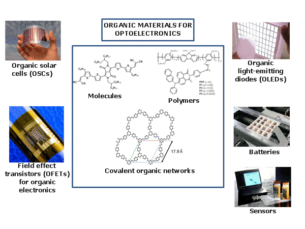
Different types of organic materials (molecules, polymers and covalent organic networks) and selected applications of them (field effect transistors (OFETs) in organic electronics, organic solar cells (OSCs), light-emitting diodes (OLEDs) sensors and batteries).
The main interest in this new technology is the notion that devices based on thin films of organic materials offer new possibilities in the field of optoelectronics, combined with the existence of a cheap technology already developed in the manufacture of light-emitting diodes Organic (OLEDs) with plastic type materials. On the other hand, the flexibility provided by organic chemistry in terms of molecular design allows access to the desired properties, such as high electronic mobility, molar absorptivity coefficient, mechanical flexibility and even color and partial transparency of the devices, this being last a possible prerequisite for the general acceptance of organic optoelectronic devices in modern architecture.
|
How does it work |
At the present time, one of the limiting factors for the use of organic materials in different optoelectronic devices is their moderate load mobility. In our research group we address the synthesis of new organic materials aimed at the optimization of different characteristics such as the levels of their border orbitals, the adequate morphologies of films made with these materials, their thermal, chemical and photochemical stability opens the way to use of these materials in different optoelectronic devices. With regard to the use of these materials for the efficient conversion of energy in solar cells, a high control over their border orbital levels allows to reach a good agreement between the absorption spectrum of the active layer and the spectral distribution of lengths of wave in solar radiation. The recent use of organic materials with a better coincidence of the absorption of the polymer with the solar emission spectrum, has been shown to be an effective strategy to increase the number of photons absorbed and, with it, the photovoltaic efficiency of the cell.
|
Advantages |
The investment in this field will allow the development of a cheap optoelectronic technology. Along with the advantages that this entails in economic terms will also achieve environmental benefits derived from the use of organic materials in photovoltaic devices.
|
Where has it been developed |
The technology has been developed in the Organic Chemistry Department of the Faculty of Chemical Sciences. The research group synthesizes new molecular organic and polymeric materials, studies its electrochemical and photophysical properties and selects the most suitable materials to be used in the manufacture of optoelectronic devices. Collaboration is sought with companies interested in the incorporation of these materials in optoelectronic devices including field effect transistors, light emitting diodes and low cost photovoltaic cells based on the use of organic materials.
|
And also |
The group has recently initiated a line of work aimed at the development of covalent organic networks (COFs) that allow the organization of organic building blocks with atomic precision to generate bi- and three-dimensional porous crystalline structures connected by strong covalent bonds. We hope that the incorporation of photo and electroactive organic units to these highly organized structures will make it possible to further improve the provings of organic materials in optoelectronics.
|
Contact |
|
© Office for the Transfer of Research Results – UCM |
|
PDF Downloads |
|
Clasification |
|
Responsible Researcher |
José Luis Segura Castedo: segura@ucm.es
Department: Organic Chemistry I
Faculty: Chemical Sciences


